A semiconductor microchip, often referred to as an integrated circuit (IC) or simply a “chip,” is a small electronic device made from semiconductor materials (primarily silicon) that integrates millions to billions of electronic components—such as transistors, resistors, capacitors, and diodes—onto a single substrate. Microchips are the cornerstone of modern electronics, enabling compact, efficient, and powerful devices.
- Purpose: Microchips perform a wide range of functions, including computation, memory storage, signal processing, and power management.
- Historical Context: The first IC was demonstrated in 1958 by Jack Kilby at Texas Instruments, followed by Robert Noyce at Fairchild Semiconductor, who developed a planar process that became the standard for modern chip manufacturing. This invention earned Kilby the Nobel Prize in Physics in 2000.
- Moore’s Law: Proposed by Gordon Moore in 1965, this empirical observation states that the number of transistors on a microchip doubles approximately every two years, leading to exponential growth in computing power. While this trend has slowed in recent years due to physical limits, it has driven microchip development for decades.
Microchip Structure/Architecture and Components
A. Transistor-Level Design
- MOSFET (Metal-Oxide-Semiconductor Field-Effect Transistor):
- NMOS & PMOS: Complementary MOSFETs form CMOS logic, the basis of digital ICs.
- FinFET (3D Transistors): Introduced at 22nm to combat leakage currents.
- Gate-All-Around (GAA/Nanosheet FETs): Next-gen transistors at 3nm and below for better electrostatic control.
- Memory Cells:
- SRAM (Static RAM): Fast, volatile memory used in CPU caches.
- DRAM (Dynamic RAM): High-density volatile memory (requires refresh cycles).
- Flash (NAND/NOR): Non-volatile storage (SSDs, USB drives).
B. Logic and Analog Circuits
- Digital Logic Gates (NAND, NOR, XOR): Implement Boolean functions.
- Clock Distribution Networks: Synchronize operations (~GHz frequencies).
- Analog/RF Circuits:
- ADCs/DACs (Analog-to-Digital Converters)
- PLLs (Phase-Locked Loops) for clock generation.
C. Interconnects and Packaging
- Back-End-of-Line (BEOL) Wiring:
- Copper (Cu) Damascene Process: Replaced aluminum for lower resistance.
- Low-k Dielectrics: Reduce parasitic capacitance.
- Advanced Packaging:
- Flip-Chip, TSV (Through-Silicon Vias), 3D ICs for high-speed interconnects.
- Chiplet-Based Designs: Modular approach (e.g., AMD EPYC, Intel Ponte Vecchio).
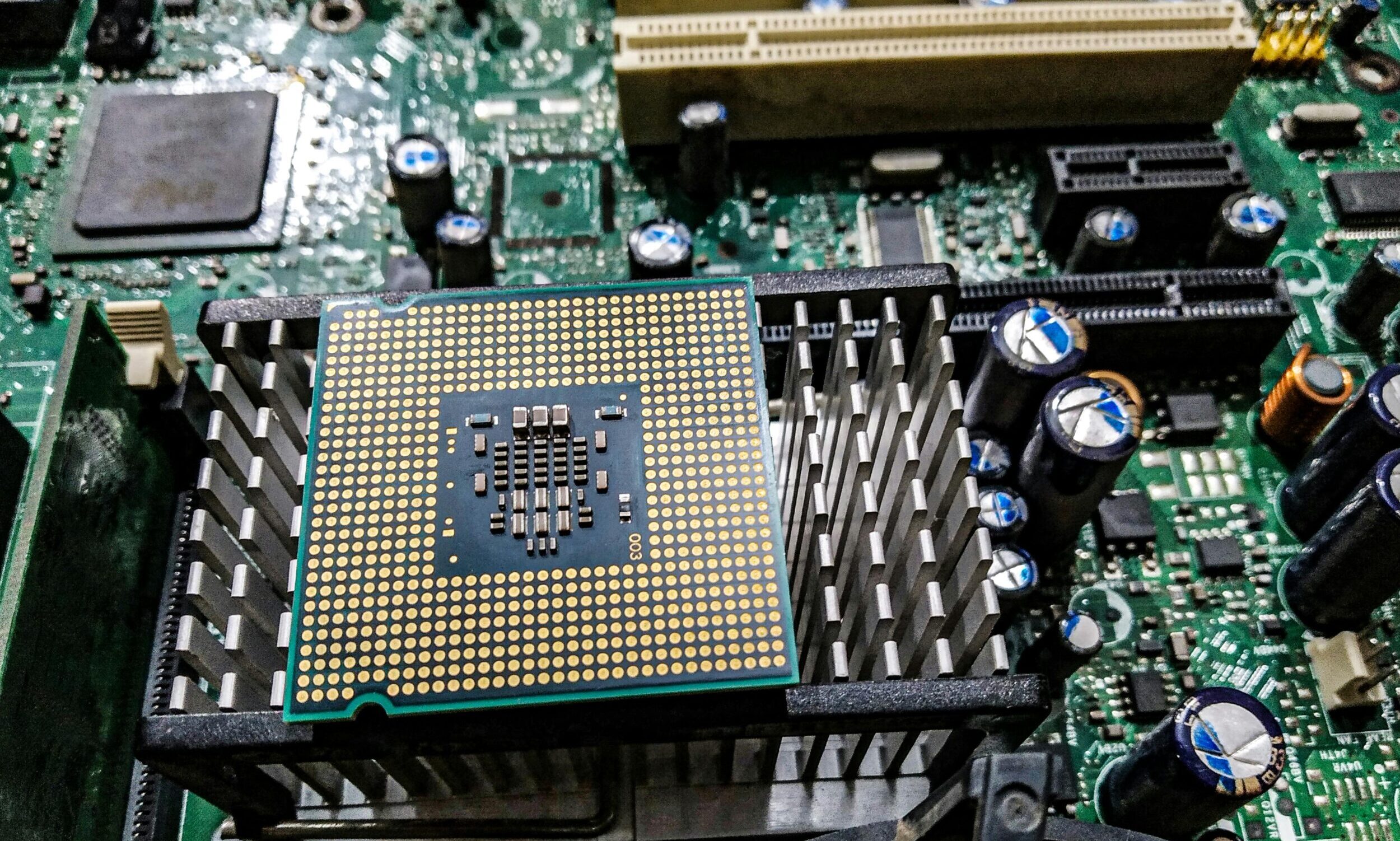
A microchip is a highly complex, layered structure built on a semiconductor substrate. Its key components include, that is we can also understand in such way :-
- Substrate:
- Typically a thin wafer of single-crystal silicon, though other materials like gallium arsenide (GaAs) or silicon carbide (SiC) are used for specialized applications.
- The substrate provides a foundation for building the chip’s circuitry.
Transistors:
- The fundamental building blocks of microchips. Transistors act as switches or amplifiers.
- Types:
- MOSFET (Metal-Oxide-Semiconductor Field-Effect Transistor): The most common transistor in modern chips, used in digital and analog circuits.
- FinFET: A 3D transistor structure introduced around 2011 to improve performance at smaller scales.
- Gate-All-Around (GAA) FET: An advanced transistor design (e.g., nanosheet transistors) used in 3 nm and 2 nm nodes for better gate control and reduced leakage.
Interconnects:
- Thin metal layers (usually copper or aluminum) that connect transistors and other components.
- Dielectric layers (e.g., silicon dioxide or low-k dielectrics) insulate the interconnects to prevent unwanted electrical interactions.
Passive Components:
- Resistors, capacitors, and inductors are integrated into the chip for signal processing and power management.
Layers:
- A modern microchip has 10–20 layers, including active layers (transistors), interconnect layers, and passivation layers (to protect the chip).
Types of Microchips
Microchips are classified based on their functionality:
- Microprocessors (CPUs):
- The “brain” of a computer, executing instructions from software.
- Example: Intel Core, AMD Ryzen, ARM-based chips (e.g., Apple M-series).
- Memory Chips:
- DRAM (Dynamic Random-Access Memory): Used for temporary data storage in computers. Requires constant refreshing.
- SRAM (Static Random-Access Memory): Faster than DRAM, used in cache memory.
- NAND Flash: Non-volatile memory for long-term storage (e.g., SSDs, USB drives).
- NOR Flash: Used for firmware storage.
- Microcontrollers (MCUs):
- Integrate a CPU, memory, and peripherals on a single chip for embedded systems (e.g., in appliances, IoT devices).
- Application-Specific Integrated Circuits (ASICs):
- Custom-designed for specific tasks (e.g., Bitcoin mining, AI inference).
- Example: Google’s Tensor Processing Unit (TPU).
- System-on-Chip (SoC):
- Integrates multiple subsystems (CPU, GPU, memory, I/O) on a single chip.
- Common in smartphones (e.g., Qualcomm Snapdragon, Apple A-series).
- Analog and Mixed-Signal Chips:
- Handle analog signals (e.g., audio, RF) or combine analog and digital functions.
- Example: RF chips for 5G communication.
- Power Management ICs (PMICs):
- Regulate voltage and current in devices (e.g., battery management in smartphones).
| Type | Description | Examples |
|---|---|---|
| Logic Chips | CPUs, GPUs, AI accelerators | Intel Core, NVIDIA A100 |
| Memory Chips | DRAM, NAND Flash, SRAM | Samsung DDR5, Micron SSDs |
| Analog/Mixed-Signal | Sensors, Power Mgmt. ICs (PMICs) | TI Op-Amps, ADI ADCs |
| RF/Wireless | 5G mmWave, WiFi/Bluetooth ICs | Qualcomm Snapdragon, Skyworks |
| ASICs/FPGAs | Custom-designed ICs | Bitcoin Miners, Xilinx FPGAs |
Microchip Design Process
Designing a microchip is a complex, multi-step process involving hardware and software engineering:
- Specification:
- Define the chip’s purpose, performance goals, power consumption, and size constraints.
- Example: A smartphone SoC might need a high-performance CPU, GPU, AI accelerator, and 5G modem.
- Architecture Design:
- Choose the chip’s architecture (e.g., RISC vs. CISC for CPUs, ARM vs. x86).
- Break the design into functional blocks (e.g., CPU cores, memory controllers).
- Logic Design:
- Use hardware description languages (HDLs) like Verilog or VHDL to describe the chip’s logic.
- Simulate the design to verify functionality.
- Physical Design:
- Synthesis: Convert the HDL code into a gate-level netlist (a list of interconnected logic gates).
- Place and Route: Arrange the gates and interconnects on the chip layout, optimizing for speed, power, and area.
- Design Rule Check (DRC): Ensure the layout adheres to manufacturing constraints.
- Verification:
- Simulate the chip’s behavior under various conditions to catch errors.
- Use formal verification to mathematically prove correctness.
Microchip Fabrication Process
Fabrication, or “fab,” is the process of manufacturing microchips in a cleanroom environment. It involves several steps:
- Wafer Preparation:
- Start with a high-purity silicon ingot, grown using the Czochralski process.
- Slice the ingot into thin wafers (typically 300 mm in diameter) and polish them to a mirror finish.
- Photolithography:
- Coat the wafer with a light-sensitive photoresist.
- Use a mask to project a pattern onto the wafer with ultraviolet (UV) light.
- Modern processes use Extreme Ultraviolet (EUV) lithography for sub-5 nm features, with wavelengths as small as 13.5 nm.
- Etching:
- Remove exposed areas of the wafer to create patterns (e.g., trenches for transistors).
- Techniques: Wet etching (chemical) or dry etching (plasma-based, e.g., reactive ion etching).
- Doping:
- Introduce impurities (e.g., boron for P-type, phosphorus for N-type) to create p-n junctions.
- Methods: Ion implantation or diffusion.
- Deposition:
- Add thin films of materials (e.g., silicon dioxide for insulation, metal for interconnects).
- Techniques: Chemical Vapor Deposition (CVD), Physical Vapor Deposition (PVD), Atomic Layer Deposition (ALD).
- Chemical Mechanical Planarization (CMP):
- Polish the wafer to ensure a flat surface for subsequent layers.
- Interconnect Formation:
- Deposit metal layers (e.g., copper) and etch them to form interconnects.
- Use dielectric materials to insulate the layers.
- Testing and Packaging:
- Test the wafer for defects (wafer-level testing).
- Dice the wafer into individual chips.
- Package the chips (e.g., in a ceramic or plastic package) and add pins for external connections.
Semiconductor Nodes and Scaling
The term “node” refers to the size of the smallest feature on a chip, historically tied to the transistor gate length. Scaling to smaller nodes increases transistor density and performance but introduces challenges:
- Historical Nodes: 90 nm (2004), 45 nm (2007), 22 nm (2012).
- Modern Nodes: 7 nm (2018), 5 nm (2020), 3 nm (2022), 2 nm (2024–2025).
- Challenges at Small Nodes:
- Quantum Tunneling: Electrons leak through thin gate oxides, increasing power consumption.
- Heat Dissipation: Higher transistor density leads to thermal issues.
- Manufacturing Complexity: EUV lithography and multi-patterning increase costs.
- Solutions:
- FinFET and GAA Transistors: Improve gate control and reduce leakage.
- 3D Stacking: Stack multiple chip layers (e.g., 3D NAND, chiplets).
- New Materials: High-k dielectrics (e.g., hafnium oxide) for gates, low-k dielectrics for interconnects.
Applications of Microchips
Microchips are integral to nearly every aspect of modern life:
- IoT & Edge Computing: Low-power MCUs (ARM Cortex-M).CPUs and GPUs in computers, servers, and data centers.
- Consumer Electronics: Smartphones, TVs, gaming consoles.(Apple A16, Snapdragon 8 Gen 2).
- Automotive: Advanced Driver Assistance Systems (ADAS), electric vehicle powertrains. (Tesla FSD, Mobileye EyeQ).
- Healthcare: Medical imaging (e.g., MRI, ultrasound), wearable health monitors.
- Telecommunications: 5G modems, optical transceivers.
- Industrial: Robotics, automation, IoT sensors.
- Aerospace and Defense: Radar systems, satellite communication.
- AI/ML: NVIDIA H100 GPUs, Google TPUs.
Recent Advancements in Microchip Technology
- Chiplet Architectures:
- Instead of a monolithic chip, use smaller, specialized chiplets connected via high-speed interconnects (e.g., AMD’s EPYC processors, Intel’s Ponte Vecchio GPU).
- Benefits: Improved yield, flexibility, and cost-efficiency.
- AI-Specific Chips:
- Chips like NVIDIA’s A100, Google’s TPU, and Cerebras’ Wafer-Scale Engine are optimized for AI training and inference.
- Features: High parallelism, low-precision arithmetic (e.g., INT8, FP16).
- Advanced Packaging:
- 2.5D Packaging: Use a silicon interposer to connect chips (e.g., NVIDIA HBM memory).
- 3D Packaging: Stack chips vertically (e.g., Intel Foveros, TSMC 3D SoIC).
- Heterogeneous Integration: Combine different types of chips (e.g., CPU + GPU + memory) in one package.
- Quantum Computing Chips:
- Semiconductor-based qubits (e.g., silicon spin qubits, GaAs quantum dots) are being developed for quantum computers.
- Example: Intel’s Horse Ridge cryogenic control chip for quantum systems.
- Neuromorphic Chips:
- Mimic the human brain’s neural structure for energy-efficient AI (e.g., Intel Loihi, IBM True North).
Challenges in Microchip Development
- Physical Limits:
- Transistor sizes are approaching atomic scales (e.g., 1 nm is just a few atoms wide), where quantum effects dominate.
- Heat dissipation and power leakage are major issues.
- Manufacturing Costs:
- Building a modern fab costs $10–20 billion (e.g., TSMC’s 3 nm fab).
- EUV lithography machines (e.g., ASML’s) cost over $150 million each.
- Supply Chain Issues:
- The global chip shortage (2020–2023) highlighted vulnerabilities in the semiconductor supply chain, prompting efforts to diversify manufacturing (e.g., U.S. CHIPS Act, EU Chips Act).
- Security:
- Hardware vulnerabilities like Spectre and Meltdown (discovered in 2018) exploit microchip designs.
- Supply chain attacks (e.g., counterfeit chips) pose risks.
- Environmental Impact:
- Chip manufacturing is energy-intensive and uses hazardous chemicals (e.g., perfluorocarbons).
- Efforts are underway to reduce the carbon footprint (e.g., TSMC’s commitment to 100% renewable energy by 2050).
Future Directions
- Beyond Moore’s Law:
- Focus on “More than Moore” approaches, such as heterogeneous integration, specialized chips, and new computing paradigms (e.g., quantum, neuromorphic).
- New Materials:
- 2D materials like graphene and MoS₂ for ultra-thin transistors.
- Carbon nanotubes for high-performance interconnects.
- Photonics Integration:
- Use silicon photonics to integrate optical components (e.g., lasers, waveguides) on microchips for faster data transfer.
- Sustainability:
- Develop recyclable chips and reduce water and energy usage in fabs.
- Edge Computing:
- Design low-power chips for IoT and edge AI applications (e.g., Arm Cortex-M series).
Semiconductor microchips are the foundation of modern technology, enabling everything from smartphones to supercomputers. Their development involves a delicate balance of physics, engineering, and innovation. As we approach the physical limits of scaling, the future of microchips lies in new architectures, materials, and manufacturing techniques. Understanding microchip technology is essential for grasping the trajectory of technological progress and its impact on society. . . Semiconductor microchips are the most complex human-made devices, pushing the limits of physics, materials science, and engineering. Future advancements in GAA transistors, 3D ICs, and quantum computing will continue to drive innovation.
References:-
- “CMOS VLSI Design” – Neil Weste & David Harris
- “Semiconductor Manufacturing Technology” – Michael Quirk
- IEEE & IEDM Conference Papers on Advanced Nodes